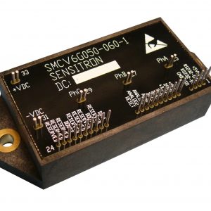
A System-In-Package (SiP) consists of a number of dissimilar integrated circuits enclosed in a single highly miniaturized package. The SiP performs all or most of the functions of an electronic system, and, it can contain several silicon components (bare die or package) and passive components.3D Plus provides a one-stop source for customer’s concept analysis, feasibility study, design, manufacturing and test of High Reliability and High Performance SiP.
Our State-of-the Art stacking technologies for SiP allow us to bring the best standard semiconductor devices and technologies in one single highly miniaturized package with almost no limit for the merging of heterogeneous technologies (Die – package – Passives).
Achieving a combination that cannot be realized with monolithic System-on-Chip (SoC) approaches, and, relying on a proven “first time right” design and development methodology, 3D Plus SiP stacks are more effective and have also a lower development cost and a faster time to market. More information
START YOUR SiP DESIGN HERE
Summarize the following information to submit your custom SiP concept analysis and feasibility study:
- Part list (final or preliminary)
- Block diagram (if available)
- Main electrical featues (voltages, currents, operating frequency, …)
- Power dissipated
- Module max size
- Module Mounting technology
- Module I/O number
- Other characteristics (environement specification, quantity, quality grade,…)